A value chain is a detailed framework that illustrates the sequence of processes involved in transforming economic inputs into valuable outputs. Each link in this chain embodies a supplier-customer relationship that lead to the final circuit board to be used in a multitude of industries, such as Artificial Intelligence, Electronics, and Electric Vehicles for example. This complex linked system occurs not only within a single organization but also across multiple entities in the market.
In the intricate landscape of the silicon semiconductor industry, the global supply chain is a vital force driving ongoing technological innovation. This complexity arises from the interconnected relationships and dependencies among various stakeholders.
Our materials serve crucial functions in the applications that comprise these linked processes. They are meticulously designed to manage the purity of critical components, ensuring their reliability and efficiency. Additionally, they significantly enhance the thermal performance of the final circuit boards, contributing to the overall efficacy and durability of electronic devices.
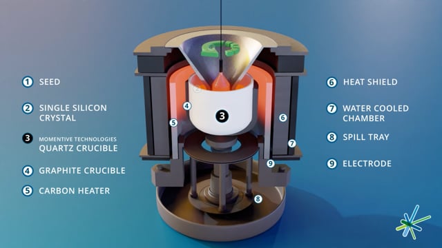
Ingot
Crystal Growth (Si)
Fused Quartz products like tubes, rods, and windows are used in semiconductor manufacturing. Quartz assemblies are used to maintain high purity during high temperature, high pressure, and vacuum processes. They also ensure that the quartz doesn’t react with the wafers or introduce particles that could cause circuit failures.
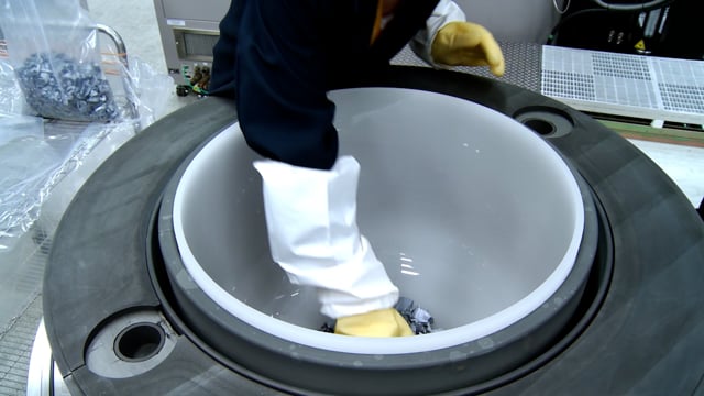
Our quartz glass crucible sets the standard for silicon semiconductor manufacturing. With exceptional purity, durability, and resistance to blowholes, it ensures flawless production of single crystal silicon, even under the toughest conditions. Built to last, it’s the key to driving innovation in tomorrow’s technology.
In-depth technical information and details for Quartz Crucibles.
Technology is constantly advancing and devices are becoming more compact. To fit chips and sensors in small spaces, reducing the thickness of semiconductor wafers is essential. Since these wafers are fragile, they need temporary stabilization for processing. By bonding device wafers to carrier wafers, they can be safely handled without damage.
In the semiconductor industry, silicon wafer carriers are predominantly constructed from fused quartz, which is celebrated for its exceptional thermal stability and resistance to chemical corrosion. Commonly known as quartz boats, these carriers are designed specifically to hold and evenly heat silicon wafers during various manufacturing processes. Their precise engineering ensures that wafers are maintained in the ideal position, allowing for uniform temperature distribution essential in semiconductor fabrication.
Fused Quartz Wafer Carrier Assembly
Fused Quartz Wafer Carrier Assembly
榴莲视频下载污黄 quartz rods are known for their exceptional purity, high temperature and chemical resistance, tight dimensional control, and mechanical strength. These qualities make them ideal for demanding applications, preserving wafer handling integrity and ensuring the quality of semiconductor chips while maintaining reliable performance.
In-depth technical information and details for Fused Quartz Rods.
Initially, a wafer is formed, which serves as the foundation for the silicon that has been carefully extracted from an ingot. This flat, circular piece can host an array of tiny circuits, all intricately arranged on its surface.
Once the wafer has been prepared, it is meticulously sliced into individual units known as die. Each die contains a complete circuit, capable of performing specific functions.
Following this cutting process, the die are packaged with precision and transformed into integrated circuits. These compact, robust circuits are essential components in a diverse range of devices, including smartphones, automobiles, computers, and countless other technologies that shape our daily lives.
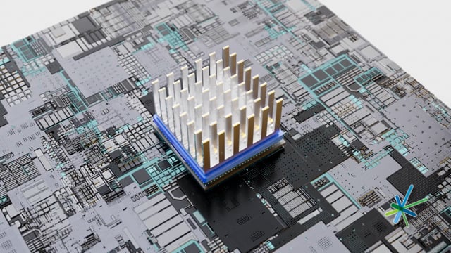
Heat poses a significant threat to today’s electronic components, reducing their service life and reliability. This challenge intensifies as designers create smaller, faster assemblies, making effective heat dissipation essential.
?
Hexagonal Boron Nitride (BN) and Spherical Alumina (SA) fillers address this issue. When added to polymers, BN and SA enhance heat dissipation, which helps improve the longevity and reliability of electronic components. Compared to fused silica, aluminum oxide, and aluminum nitride, BN and SA excel in thermal conductivity, with some composites achieving levels as high as 15 W/mK.
In-depth technical information and details for Boron Nitride and Spherical Alumina.
Heat is one of the major threats to today’s electronic components and assemblies. It can shorten their service life and compromise reliability. As designers and manufacturers strive to create smaller, faster assemblies, the need for effective heat dissipation becomes increasingly important.
Hexagonal Boron Nitride (BN) fillers offer a solution. When incorporated into various polymeric materials, BN’s heat-dissipating properties help extend the service life and improve the reliability of electronic components and assemblies.
In-depth technical information and details for Boron Nitride and Spherical Alumina.
Semiconductor chips are crucial in many applications, including smartphones, computers, TVs, automotive systems, medical devices, and industrial machinery. They control the flow of electrical current, making them essential for nearly all modern electronic devices.
Electronics
Medical Devices
Household Appliances
Key application areas of semiconductor chips:
Consumer electronics like mobile phones, laptops, game consoles, microwaves, and refrigerators depend on semiconductor components. The high demand for these devices has led to long wait times for many products.
Embedded systems are small computers integrated into larger machines, controlling the device and enabling user interaction. Examples include central heating systems, digital watches, GPS devices, fitness trackers, televisions, and vehicle engine management systems.
Silicon is the most commonly used semiconductor for manufacturing solar panels.
Products Used in Silicon Semiconductor Processes
Quartz
Crucibles
Ceramics
Have questions or need more information about how we assist customers in thinking big with their semiconductor innovations?